
It is a normal development log.
Rev 01
2021-09-24
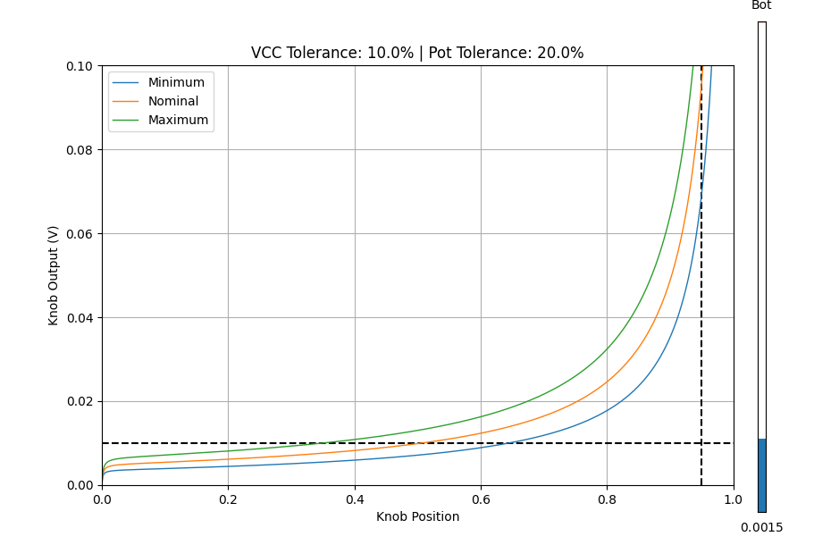
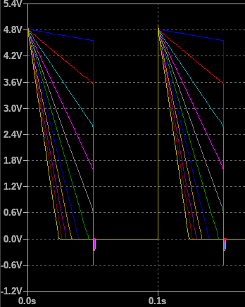
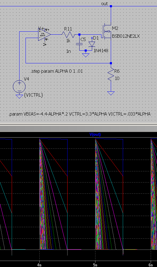
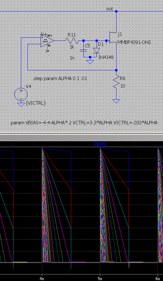
Variations by +/- 20% in the maximum potentiometer resistance have a dramatic effect on the filter behavior at long decay times, as they shift the minimum control voltage:
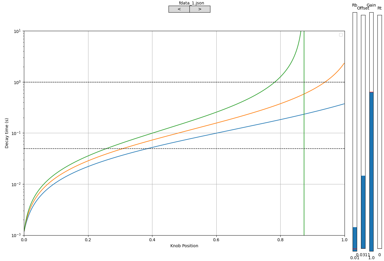 This can to some extent be compensated by adjusting the offset, though it doesn't fully compensate for variation at shorter decay times.
2021-09-23
Developing a simple curving circuit that maps knob position into control voltage to give useful control over decay times in both the ranges 1 ms to 50 ms and 50 ms to 1-10 s has proven difficult. In the case where 3.3 V maps to the minimum decay time of 1 ms, the corresponding control voltages for the breakpoints of 1 ms, 50 ms, and 5 s are 3.3, V, 71.8 mV, and 718 uV respectively. Simple piecewise-linear op-amp circuits require breakpoints in excess of 0.5 V or so. It's possible to achieve better control over the audio frequency cutoffs by applying a small negative offset to the knob control voltage, but this causes the envelope-rate control to become super-exponential rather than linear, which is not desirable.
It seems that with simple well-behaved circuitry, the goals of having good control over audio rates and envelope rates are mutually exclusive. Software could map the knob position value to a control voltage relatively easily, but would require pins I don't have to spare. I also don't know if the PWM-style DAC functionality available on the teensy can achieve the necessary voltage resolution (> 12-bit) to control the filter. There might also be a conflict between the existing clock frequency control configuration and higher resolution PWM configuration.
Another option is to relax the requirements for the filter control. Linear control from 1 ms to 1 - 10 s is achievable. If the audio-frequency cutoff configuration is taken as a binary on/off AC coupling mode rather than a continuous tone control, then it's not too hard to make one extreme of the knob give a high cutoff frequency while the rest of the knob controls decay time and acts like DC-coupling.
On the other hand, precise control of decay time could be eliminated in exchange for better audio-frequency control using the previously mentioned negative offset. There would still be some envelope decay control, especially in the range of about 100 - 500 ms, but longer decay times would be difficult to configure reliably. As much as I like the idea of having easily controlled envelope-like functionality for pseudorandom rhythm generation, I don't think it's a feature that will get used a lot compared to the normal oscillator operation, so it might make sense to sacrifice envelope-rate control for audio-rate control.
I would like to be able to tune the knob-voltage-t0-control-voltage gain to compensate for variation in filter capacitance, and I'd also like to be able to tune the offset voltage to adjust the maximum achievable decay time of the filter. This may require a additional buffering to make the two controls independent, which is unfortunate. I could use the op-amp currently serving as a comparator, but then I lose bypass functionality, which may be necessary with a low maximum decay time to allow for rhythm-rate logic signals.
Alternatively, I might introduce a dedicated 2-channel comparator to both enable bypass mode and provide hysteresis on the external clock input.
2021-09-19
Given that the constant current filter implementation yields a perfect inversely proportional relation between decay time and control voltage, it is possible to perfectly linearize the relation between knob position and decay time. If the knob serves as the variable top leg of a voltage divider with a fixed bottom leg, then the divider ratio can be represented as 1/(1+a) where a is the ratio of the knob resistance to the resistance bottom leg, and ranges from 0 to the maximum knob resistance. Then, since the decay time is given by T = k/VCTRL, this gives T = (1+a)k. k here is the minimum decay time achieved when the knob is at 0%, yielding the maximum possible control voltage. (1+a) gives the dynamic range of the filter decay time, i.e. the ratio of maximum to minimum decay time.
This is, unfortunately, and undesirable implementation. If the minimum decay time is 1 ms (limited by the resistance of the sense resistor and minimum rdson of the NFET), and the maximum decay time is 10 s, then a is 9999. For a 100k potentiometer, this means the bottom leg of the divider is 10 ohms, and in the worse case will draw 330 mA from a 3.3 V supply or 10 mA from a 100 mV supply (100mV being the maximum useful control voltage in the current implementation). Additionally, the range of the knob that yields audio-frequency effects (estimated as a decay time of 50 ms or less) is 0% to 0.5%, so while this configuration yields perfect linear control of envelope-like behavior, it yields no control of audio-frequency filtering. Even dropping the maximum decay time all the way down to 1 second brings the audio-rate range to 5% of the knob range.
I would like to try modifying the filter to add some gain to the current sense signal, but unfortunately this would require lifting a pin on the other op-amp to reconfigure it as a non-inverting amplifier. I may try that anyway. Another option might be to try to breadboard a solution, which could also be useful for iterating on different knob to voltage mapping schemes. I'm not too keen on that approach since I'd have to get power supplies onto the breadboard and route a lot of wires to the PCB (plus I don't have any through-hole TL072's, and I'm not sure that the breadboard itself wouldn't introduce issues).
2021-09-18
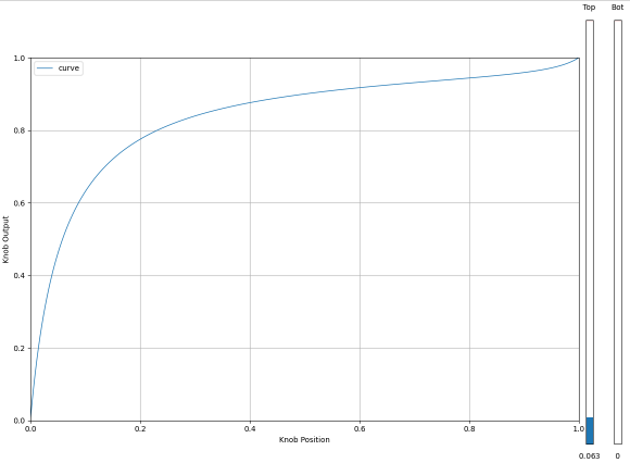
Selecting 10 mV pre-divider control voltage as the nominal 50% point as a starting point based on yesterday's data, I get the following potentiometer curve
There are a few potential concerns with this method.
- The knob voltage doesn't get very close to 0 over most of its range, which could limit the maximum achievable decay time in the useful tuning range
- In particular, the control voltage only gets as low as about half the 50% voltage, which should correspond to just twice the decay time.
- A 1-second decay time at 50% then yields a maximum of 2 s decay time.
- The curving resistor is just 150 ohm. In the worst case, this will draw 22 mA of current and dissipate 72.6 mW, which exceeds the power rating of a 1/16 W resistor.
I don't have a 150 ohm resistor on hand, so I might use two 249 ohm resistors in parallel to handle the high power dissipation. This will shift the curve a little lower than nominal, but should be fine for initial characterization especially given that my baseline estimates aren't very good.
I'm not sure that I'll be able to effectively measure the control voltages involved in the current configuration. It might be worthwhile to add some gain to the current-sense feedback so that I can use higher control voltages. This could allow for a larger potentiometer curving resistor with better dynamic range. The main concern would be error or delay added to the measured current signal by the amplifier. In simulation, this appears to introduct some instability that prevents the simulation from completing.
With the ~125 ohm curving resistance in place, I see decay times of roughly
| Knob Position (%) | Decay Time (ms) |
| 0 | N/A |
| 25 | 1800-2100 |
| 50 | 750-810 |
| 75 | 260-350 |
| 100 | 1.15 |
I'm really just eyeballing the knob positions here, so it's not necessarily consistent or accurate. I've able to select decay times up to 8 seconds, which is a good sign. It's a bit fiddly at that point, but it's still well above the minimum knob position, and with < 1 s at 50%, this curve seems to yield better dynamic range than predicted.
The range of audio-frequency cutoffs (<20 ms decay time) is almost non-existent, though, falling somewhere in the last 5-10 % of the knob. I may be able to afford a less drastic curve to gain more access to the audio range of cutoff frequencies while losing the more extreme decay times. The 1-second decay mark will shift even further left on the knob, but as long as it's still accessible I think that's probably fine.
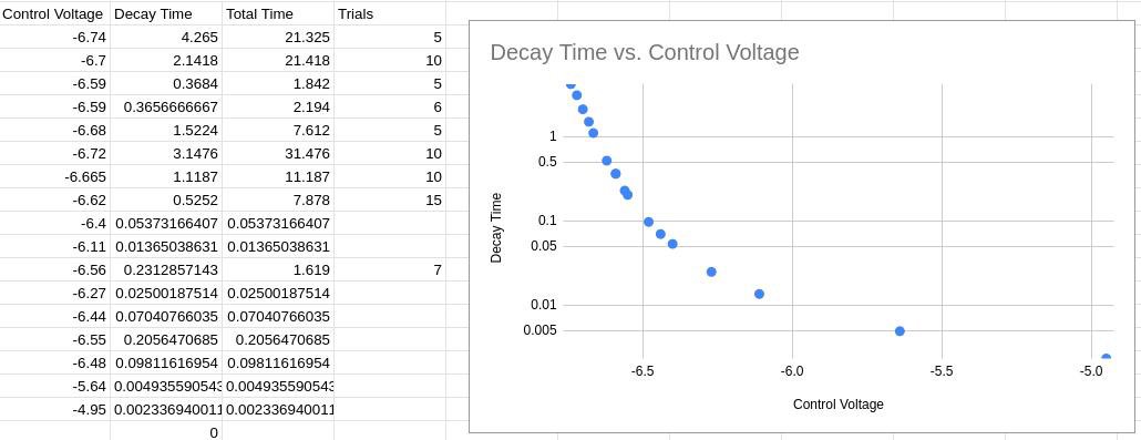
The external clock has suddenly become very unreliable except when I flip it over and try to debug it. Possible a bad solder joint somewhere in the mod. I was nonetheless able to take some measurements, and I'm surprised at how clean the data looks. Though there is substantial error in the ES-8 control voltage measurements, it was nonetheless able to differentiate variation of less than 1 mV, showing a clear linear relationship between control voltage and inverse decay time.
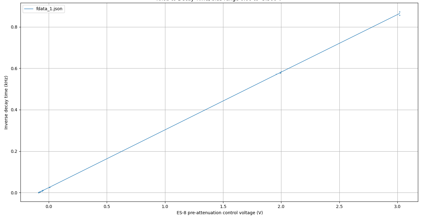
This is exactly the behavior we would expect given a current directly proportional to control voltage - T = CVpeak/I or 1/T = I/(CV). The data seems to indicate a slope of about 2.9e6 Hz/A (864 Hz over 9.6 mA). Assuming about 1.4 V of change between the peak and the end of the measurement, this corresponds to a capacitance of 245 nF, which is quite a bit lower than the 10 uF I expect. I'm not sure how to account for this yet.
Incidentally, while testing audio rate filter effects, I had changed the sequence length to maximum, which accounts for the inconsistent clocking I observed later.
2021-09-17
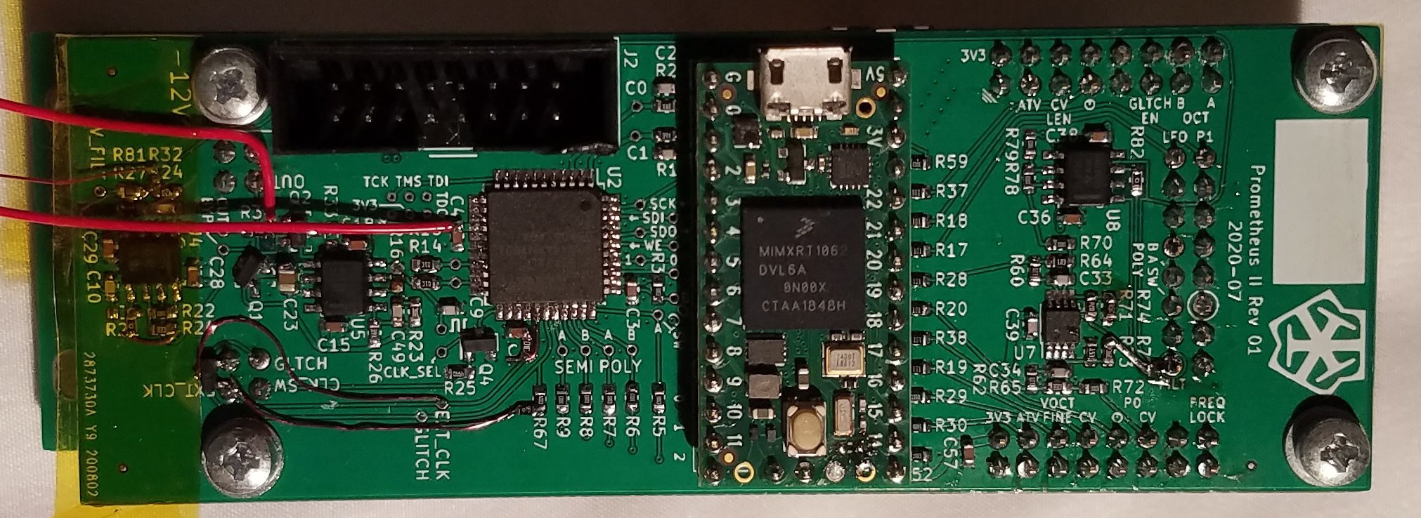
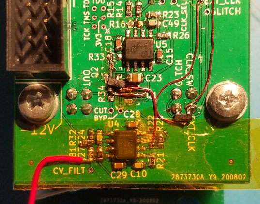
Here's a photograph of the state of the PCB at the end of yesterday's work:
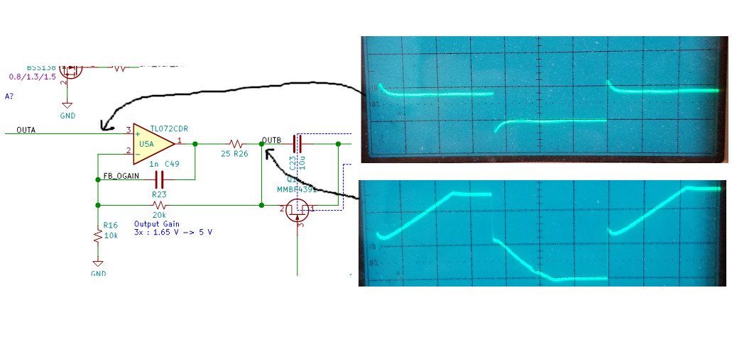
The current layout isn't ideal for implementing the constant current filter topology. The non-inverting input, which needs to be connected to the control voltage, is currently connected directly to ground, and so would have to be lifted off the pad. On the other hand, the op-amp originally used for the bypass comparator has both inputs available and is currently not in use. I would need to either cut a trace or remove the FET presently installed on the bypass FET footprint, but that should be doable, especially since the constant current implementation may not require a bypass FET at all.
The knob CV needs a lot of attenuation. In simulation, it looks like it should not exceed about 80 mV. at 100 mV there is some oscillation on rising edges that might be the beginnings of instability. I wouldn't might seeing what actually happens at 100 mV, though. I'll need attenuation by a factor of about 0.0305 to produce a 100 mV range from 3.284 V. A 1.5k and 47.5k resistor produce a voltage divider with gain of 0.306, which is pretty close.
I can reuse the NFET currently placed on the bypass FET pads as teh current sink FET by lifting one pad - the drain and gate are already in the right place. I can actually use the current CV gain amplifier for its virtual ground to create the voltage divider using existing pads. It seems a little silly, but it should work just fine and will make the reword easier.
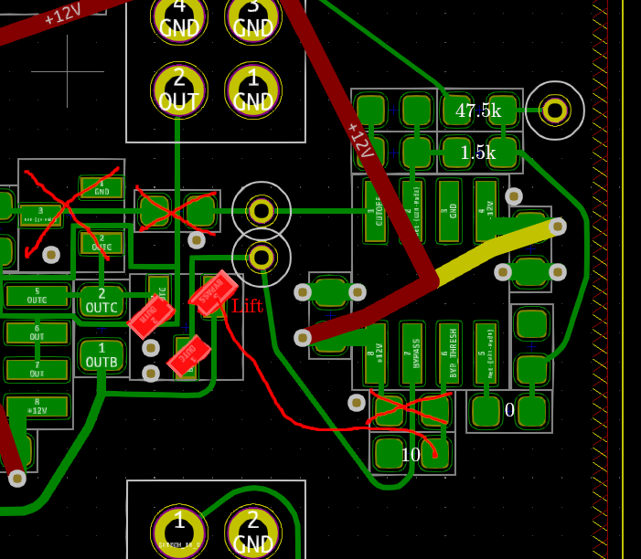
As before, I'll want to characterize filter decay time against control voltage. In this case, I'll want to measure the control voltage from the knob rather than at the op-amp input, as 100 mV will be difficult to measure accurately. To that end, I'll measure the divider resistors beofre placing them to get a more accurate estimate of the gain mapping knob voltage to control voltage. Ultimately I expect to apply a similar parallel resistor curving strategy, but with the resistor on the bottom leg of the potentiometer instead of the top since lower control voltages correspond to longer decay times.
I was mistaken about the orientation of the NFET source/drain, and I also didn't notice that the 47.5k bin was empty. I wound up using a 47k resistor.
The divider resistors measured 1.499k and 47.0k, yielding a gain of 0.03090785.
Here's the PCB after this mod:
The first thing I notice is that I connected the control voltage probe to the wrong pad, and it's reading the divided voltage instead of the knob voltage.
The maximum decay time is much shorter than I'd prefer. With the knob at 0%, I see somewhere around 70 ms. The waveform itself has a nice linear slope. If I short the control voltage input to ground at the op-amp, I can get a much longer decay time - too long to measure with the minimum internally-generated frequency. With an external clock, it is somewhere in excess of 15 seconds - my hand slipped during the measurement, but it had not decayed by much, so this is certainly a viable circuit.
Here are some captures of the waveform in the current configuration with a 100 Hz clock:
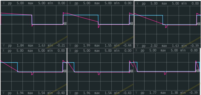
In this configuration, the minimium decay time is about 1.16 ms, and the maximum is around 61.2 ms.
I also find that if I short the buffered CV output directly to ground (with the CV to 0 V), then filter decay time increases, which suggests to me that the CV buffer may be adding some very small offset. This might also be a consequence of the virtual ground that I'm referencing my divider to having some offset. If I short the virtual ground to actual ground, then I also see the decay time increase, so this seems likely to be the case. This implies that I need to reconfigure the circuit to use a real ground for the divider.
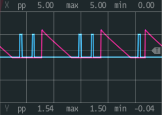
The the divider referenced to a real ground, it is possible to get a 1 s decay time, but very difficult in the current configuration. The VCV rack CV measurement is -0.088 V which is maybe 5-10 mV in real life. This is now before the divider, and so corresponds to a control voltage around 150-300 uV. At -0.078 V, the decay time is closer to 300 ms. At -0.093 V (the lowest position of the knob, or 0 V in real life), the decay time is too long to reasonably measure. Some curving will likely be necessary to characterize the filter.
Here's an example of a 1.3 s decay time with a nice linear ramp:
2021-09-16
For my future reference, I have 1.5k resistors in stock, and with a 1.5k curve resistor I would like a maximum bias of -6.5075 V and an offset of about -0.427 assuming perfect tolerance in the filter knob. In the case of poor tolerance, bias offset needs to adust from -0.439 to -0.412 V. Using a 3.3 V reference, the offset gain needs to be adjustable from at least 0.1248 to 0.1330. If I leave the 100k feedback resistor in the current circuit, then the knob input needs to be 50k, which I have, and the offset input needs to range from 750 to 800k, which I don't.
If I instead drop the feedback resistor to 47k, then I need a 22k input resistor for the knob should be adequate, and the offset input resistance needs to range from 350 to 376k. I can achieve that with a 300k resistor and a 100k pot.
I made a sign error. Actually I need to adjust the bias voltage by +0.427 Vin this configuration, which is not possible with a positive voltage reference. If I just drop the bias gain enough to allow for a negative offset, then I need more like
| Curve Resistor | Bias Gain | Bias Offset |
| 1.8k | 1.6 | -0.77 |
| 1.7k | 1.75 | -0.293 |
| 1.69k | 1.76 | -0.276 |
I have a 1.69k resistor on-hand. I measure my 3.3 V rail at 3.284 V. To obtain a gain of 1.759 or lower, I require an input resistance of 26.7k or greater. I don't have that on hand, but I do technically have a spare 500 ohms in series with the input resistor, and I could replace that with a 4.7k resistor to obtain 26.7k. Over 20% variation in curve resistance, the bias offset in this configuration ranges from -0.288 to -0.268 using 10 s at 95% as the target. Using 1 s at 50% as the target, it ranges from -0.25 (max 6 seconds) to -0.31 (max somewhere above 14 s). Finally, this yields an input resistance range for bias offset control of 497k to 617k, a range of 119k. The narrower 10 s reference range is 536 to 576. I currently have 360k on the pcb with wires breaking out to a breadboard, so I can simply add 120k on the breadboard to get a range from 480 to 580k.
Well, my 120k bag actually has 12k resistors in it. Or I misread the cards. It has been a while. In any case, even that was too much. With only the fixed 360k resistor in place, I get a maximum decay time of about 7 seconds at 100% on the knob, which gives 360 ms at 50%. 1 second sits somewhere above 75%. It's not too hard to dial in though. Just using it as an envelope and listening, the decay times I'm getting seem alright. With a sequence length of 2, if I drive the external clock with a steady 2 Hz (60 bpm) or 4 Hz (120 bpm), I can adjust the decay time by ear relatively easily.
As for audio-rate filtering, the range that produces audible variation is pretty narrow - maybe the first 5% of the knob. There is some visually-interesting variation in the harmonic content of the waveform due to the asymmetry introduced by the filter. The below spectra are a C2 with a sequence length of 2 (i.e. a square wave with 50% duty cycle as input).
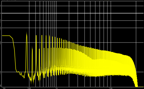
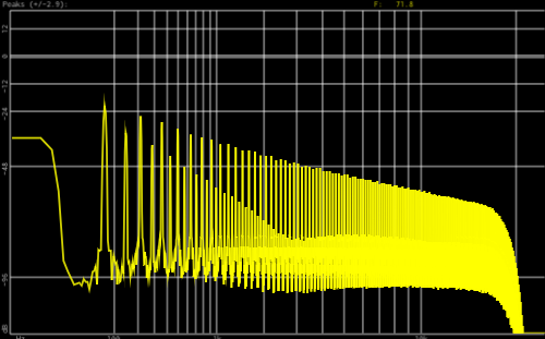
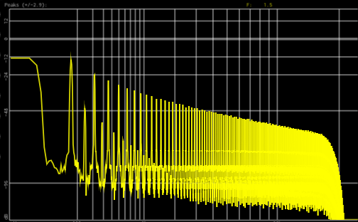
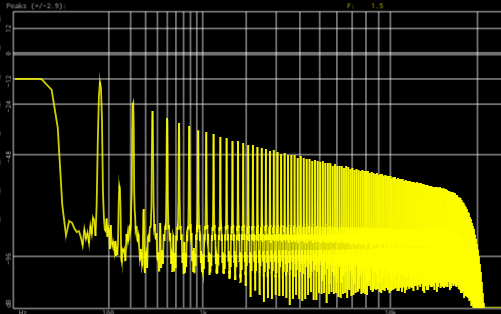
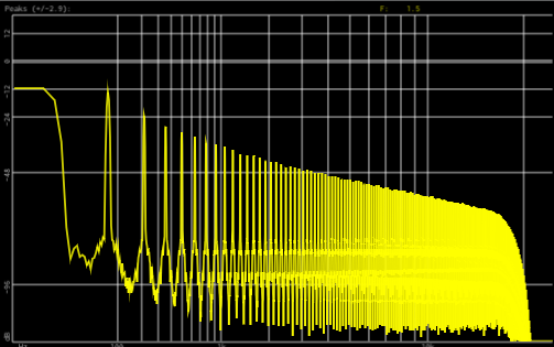
The knob positions are rougly 0, 10, 25, 50, and 100%.
Audio recordings of the filter swept over its full range with tones of a few different octaves and with one or both LFSR's enabled are here and here.
2021-09-15
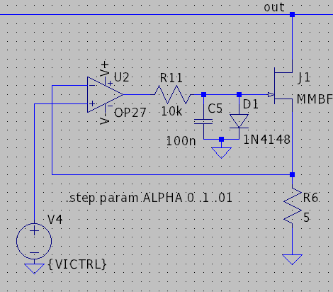
I am kind of curious about the potential for a current-regulating feedback solution to eliminate the effects of FET-to-FET variation. Basically, a small current sense resistor would be placed on the source of the JFET, and then a standard current-regulating op-amp feedback circuit would attempt to draw a fixed current through the JFET by controlling the gate voltage to set the source voltage.
There are a few potential issues with this approach:
- When the filter output drops to 0, there will be no current through the JFET, and the op-amp will drive the gate voltage as high as possible to try to compensate.
- When the next edge arrives, the JFET will be sitting at its lowest possible rds until the op-amp has time to slew all the way from its maximum output voltage down to the appropriate negative gate bias voltage.
- Placing > 0 V on the JFET gate will forward bias the junction. A resistor and schottky diode can clamp the gate voltage to prevent this, but this will in turn reduce the maximum gate bias voltage slew rate by creating an RC circuit with the gate capacitance.
In simulation with an OP-27, this seems to more or less work, though you can see the effects of limited slew rate at higher current set-points.
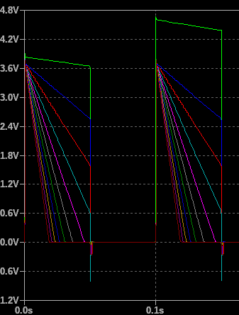
Dropping the gate capacitance to 10 nF yields much better performance. The circuit also seems to work well with the questionable TL072 model I'm using, so it might be worth investigating in hardware.
Note that in the above simulations, the control voltage ranges from 0 to 100 mV, or 0 to 20 mA through the 5 ohm sense resistor.
This approach produces a maximum decay time at 0 V control voltage, and in simulation this corresponds to about 2 seconds, which is quite a bit short than I can achieve right now. The maximum decay time can be extended some by increasing the sense resistances, though this also reduces the maximum current that can be drawn from the capacitor and therefore increases the minimum decay time.
This is probably a situation where I would want to carefully select an op-amp for high slew rate, fast recovery time, and low input offset voltage, but I'd rather avoid getting another part number involved.
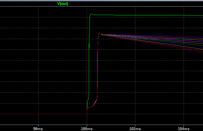
I also observe diminishing returns with a higher sense resistance, which a maximum decay time somewhere around 3.75 seconds using a 100 ohm sense resistor. When the filter output voltage drops below the current control set voltage, the op-amp circuit loses the ability to correctly regulate current, and increases the gate voltage as much as it can, reducing JFET rds to the minimum possible value and dropping the filter output all the way to 0.
In the above plot, the green traces are the filter outputs, and the blue traces are the sense resistor voltage. The horizontal axis is 4 ms/div. Not also that there is substantial ringing on the sense voltage at the edge. This circuit may be prone to instability.
My simulation still had a 100k resistor to ground on the filter capacitor output, which was causing the observed maximum decay time and exponential shape.
In simulation, the JFET can be replaced with an arbitrary NFET (and the clamping diode removed) without substantially changing the relationship between decay time and control voltage.
The NFET seems a little more well-behaved in some ways. Using a JFET, filter output voltage doesn't drop below 20 mV for some decay times, while it always gets all the way to 0 with the NFET. Naturally it would be preferable to use a cheap and widely available NFET over a JFET. I'd like to test the filter with the previously determined pot curving solution to see how it feels and sounds before tearing things apart to try this approach.
2021-09-14
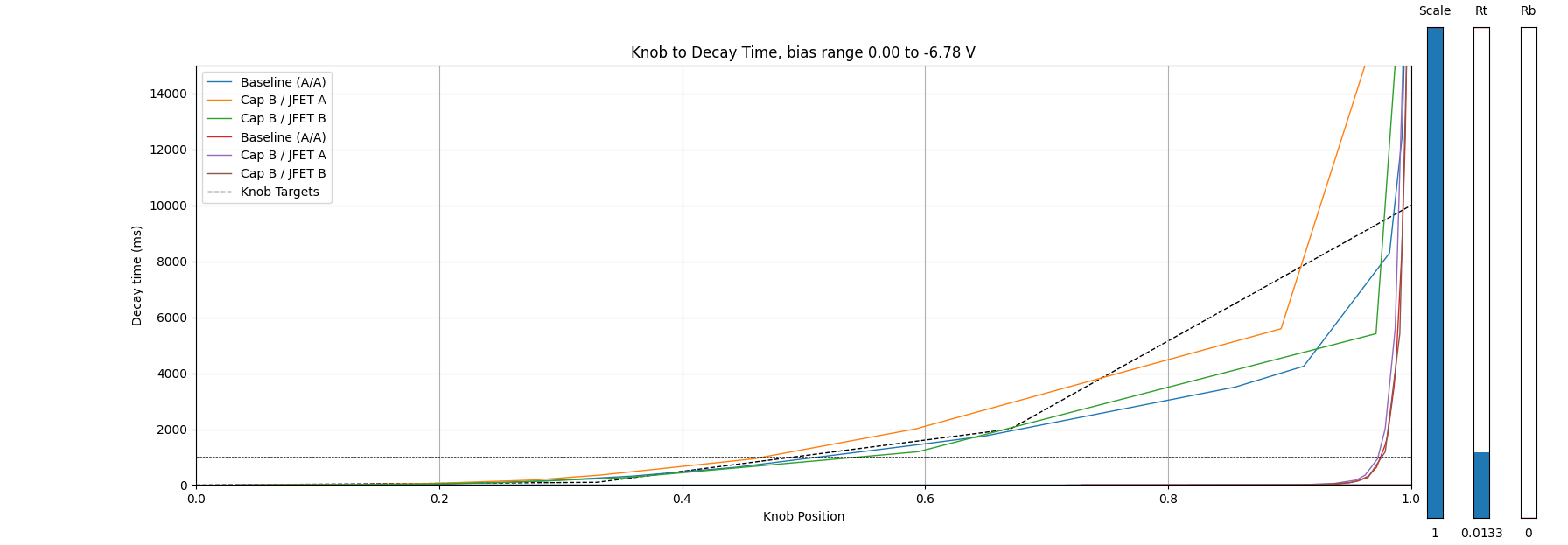
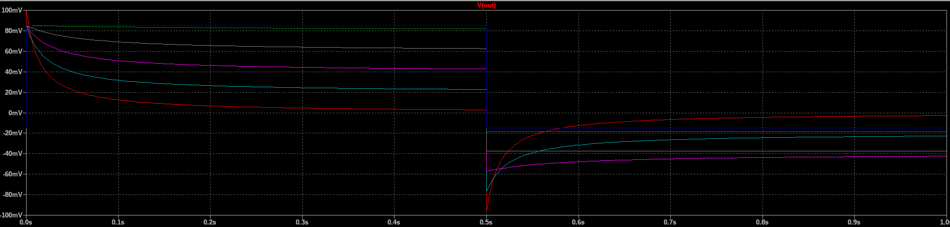
The filter knob definitely needs a buffer, as the relatively low input impedance of the inverting amplifier that produces the bias voltage will have the effect of placing a resistance in parallel with the bottom leg of the potentiometer. Also, pontentiometer tolerance matters in this application, as it affects the ratio of the curve tuning resistance to the potentiometer resistance.
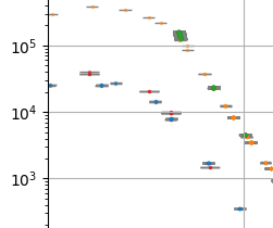
Given suitable values of bias gain and knob curving resistance (Rt), it may be possible to calibrate the decay knob by adjusting only the bias voltage offset. In the below plot, all 4 data sets have the same Rt and Max Bias, but have been tuned to different offset values. The 'Cap B / JFET B 2' dataset was taken today and separated from the original dataset since the two didn't seem to match well. I'm not sure what caused the change, but I would guess a thermal effect on the JFET threshold voltage or some other parameter.
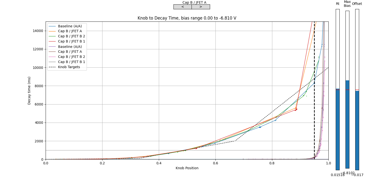
The B/A and B/B 1 curves both lack data around 10 s decay time, so I guessed at thir calibration based on the other curves and the 1 second decay time crossing. The baseline Rt and Max Bias values were selected for the Baseline curve with no bias offset. Offset voltages ranged from -17 mV to +20 mV, although the JFET B curves also include an additional 730 mV offset.
Even with +/- 20% variation in Rt, using offset to set the 95% decay time to 10 s yielded a 1s decay time withing the 40 - 60 % range for the B/B 2 data. Leaving Rt fixed, it was possible to compensate variation in max bias from -7.15 to -6.5 V without substantial variation in the curve shape, suggesting that the bias gain adjustment may not be necessary at all. With +/- 20% variation in Rt, compensating extremes in Max Bias still yielded 1-second decay times within the 40-60% range.
This seems to suggest I may be able to reduce calibration entirely to bias offset compensation, though that may still require two separate potentiometers to achieve ~1-10 mV precision with a range on the other of 1000 mV.
It seems like adjusting Rt with Offset compensated to produce maximum decay time of 10 s has the effect of shifting the 50% decay time up and down, which seems to suggest I stumbled on the ideal Rt of 0.015 purely by accident.
2021-09-13
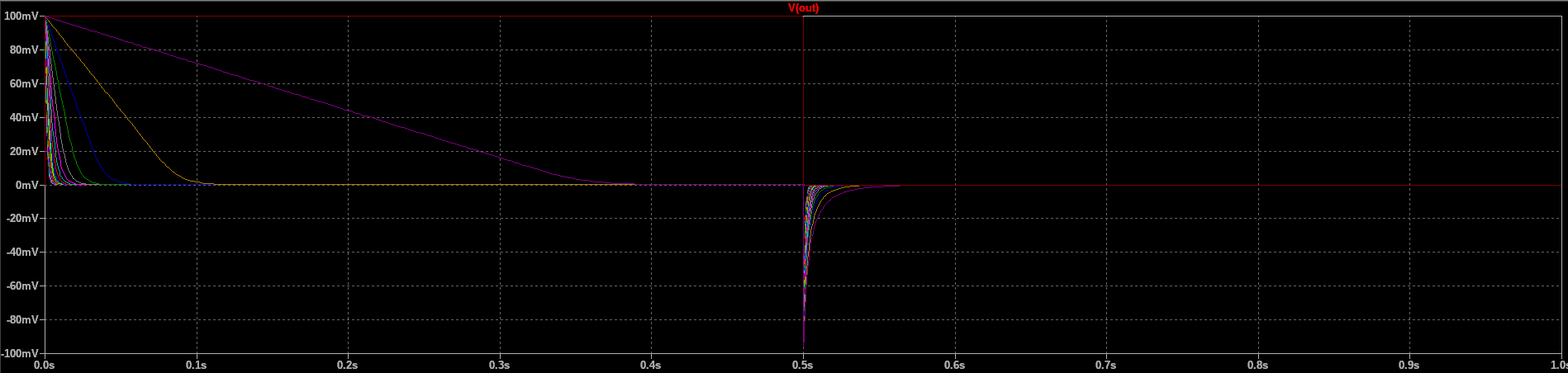
It might be okay to just add a resistance in parallel with the top leg of the filter control knob. A sufficiently small parallel resistance yields a reasonably logarithmic curve.
This in turn yields a decent-looking response in the range of 0 to 2 seconds after some tuning:
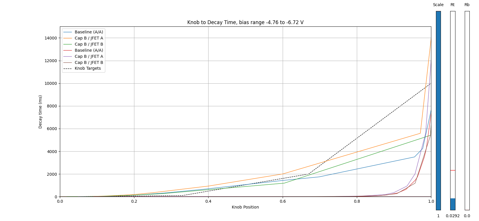
This even holds up over a wide range of biases:
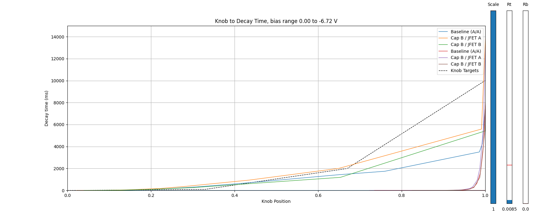
The above plots also include the decay times with the current uncurved knob implementation (in red, purple, and brown).
Even with bias all the way down to 0 V, the 1 s decay times on the curved knob fall within +/- 10% of center over variation in capacitance, with is pretty good. This is not a precision instrument. It just needs to be adjustable.
Minute variations in the peak bias voltage (e.g. by 1%) at maximum knob scale can have a pretty significant impact on the curve, requiring the parallel resistor to be adjusted some, but it's still possible to obtain adequate performance:
One drawback of this method is that there isn't really a simple calibration procedure. There are three tuning points: the bias offset, the max decay bias, and the knob curve resistor. In simulation, I've already tuned the bias offset based on my measurement data, and once its set it shouldn't really need to change. The other two parameters affect both the minimum and midpoint decay times and so can't be tuned independently. It'll have to be an iterative process. In production it may be possible to take test data and use it to generate calibration parameters. The maximum voltage generated by the knob depends on the microcontroller's 3.3 V supply, and so will be subject to some variation. Also, the knob switches over to DC coupling at the last 5% or so, and the knob's divider ration at 95% depends on its curve.
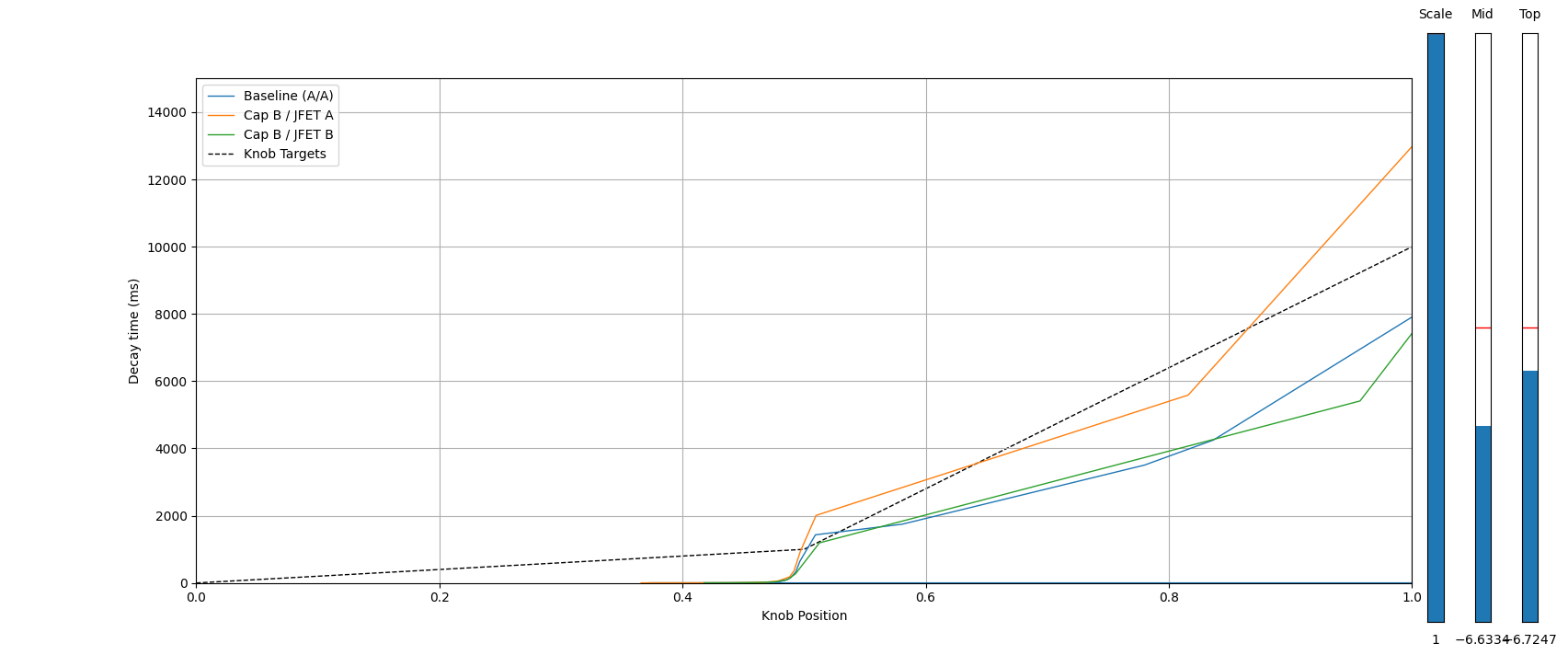
Using sliders on plots of the data I can incrementally tune the knob curve resistor and maximum bias voltage so that each of my measured decay rate curves crosses 1 second around 50% and 10 s around 95%. The parameters I got are
| Cap/JFET | Curve Resistor | Max Bias Gain |
| A/A | 0.016 | -2.06545 |
| B/A | 0.0143 | -2.05467 |
| B/B | 0.0143 | -2.06106 |
Note that the curve resistor is given as a ratio of the knob's total resistance, so 0.016 for a 100k knob is 1.6 k. Max bias gain is computed relative to 3.3 V and varies by about 0.5% at most. This will also need to be tuned to compensate for an unknown tolerance in the 3.3 V level.
I should drop the filter knob buffer from the top of the module and appropriate it for buffering v/oct CV, which needs it more anyway. I can add filtering to the bias voltage to deal with any noise that gets coupled in. Since the AC/DC comparator is already referenced to 3.3 V, I shouldn't encounter any new difficulties placing all three calibration potentiometers at the bottom of the module (especially after bumping up to 10 HP).
I may also be able to drop the knob curve tuning entirely if I'm willing to just accept 1 s of decay time falling somewhere between 40 and 60 %. This might require more detailed data with a wider range of coupling capacitors to be sure, though. It comes close with the existing data.
2021-09-12
Nothing too productive today. Mostly just noodling around with mapping bias to knob position in different ways. A simple piecewise mapping might be more or less suitable
In this configuration, the first half of the knob seems to more or less linearly control inverse decay time (i.e. frequency), while the second half gives adequate control over decay time. I'm not sure how tunable the actual piecewise mapping circuit will be, though, and the behavior is pretty sensitive to capacitor value here. Below the knee, there is no control over decay time, so the knee would probably need to be placed at a shorter decay time than 1 second in order to get good control around 1 second. Doing so might make the longer decay times harder to control, though. It might be worth considering a multi-point piecewise function depending on what tuning looks like.
I also looked at logarithmic mapping (no pictured) and it seemed to give okay results, but I don't really want to deal with translating that to a logarithmic amplifier.
2021-09-10
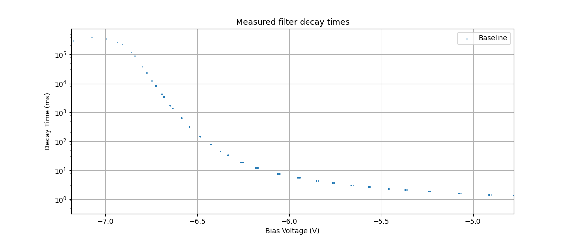
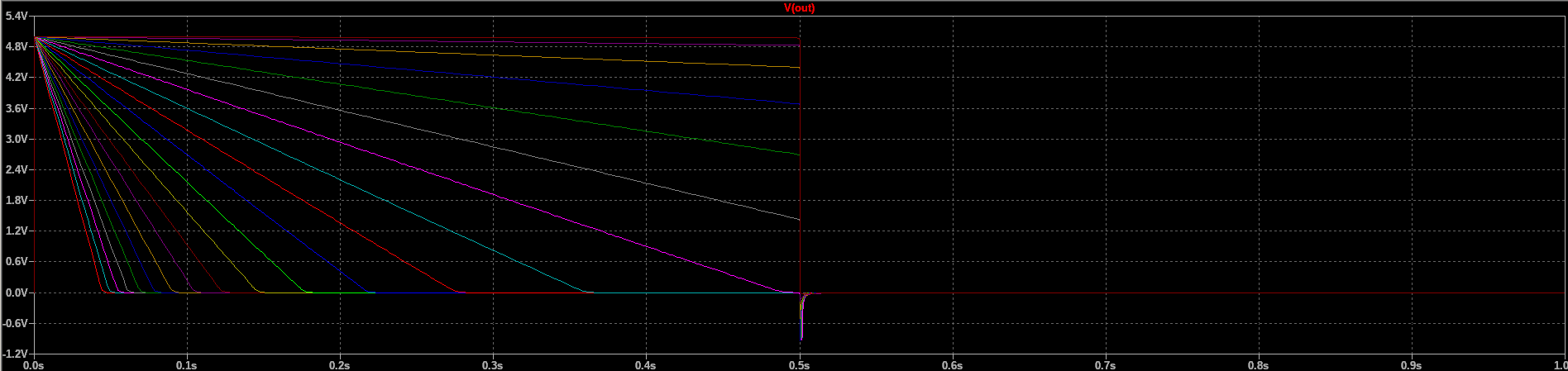
It will come as no surprise that part-to-part variation in both the filter capacitor and the JFET produce measurable variation in filter behavior.
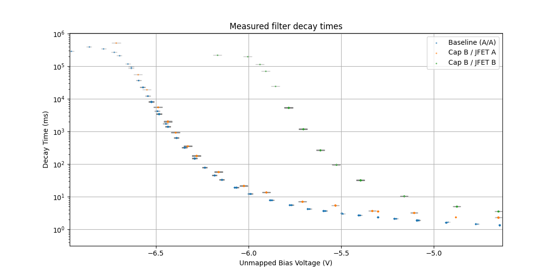
The change of JFET in particular dramatically impacts performance. We expect variation in the capacitance of the filter capacitor to produce proportional variation in the decay time of the filter, so it should be possible to scale the measured decay times in order to make the plots agree when the capacitor changes. We expect the JFET threshold voltage to vary from part to part, and since rds is a function of (VGS - Vth), we expect that it should be possible to add an offset to the bias voltage in order to compensate and make the plots agree when the JFET changes.
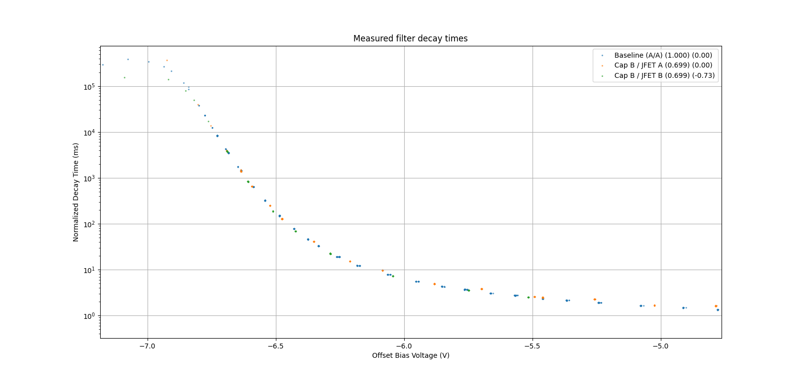
This is exactly what we observe. There is also some variation in the maximum achievable decay time between JFETs.
It should be pretty easy to calibrate out the JFET threshold variation by simple changing the offset applied to JFET bias voltage. Compensation for capacitance variation will probably depend on how the knob position ulimately gets mapped to bias voltage. Mitigating variation at the part level would require either binning parts in-house or using a part with better tolerance (like a <= 10 nF np0, producing a maximum decay time somewhere on the order of 150 ms).
2021-09-09
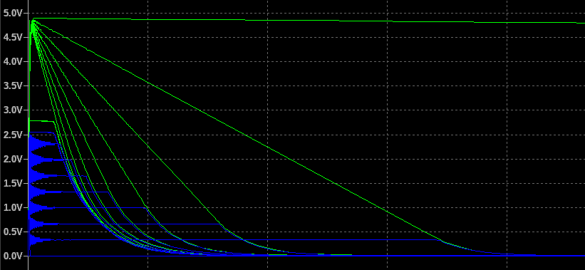
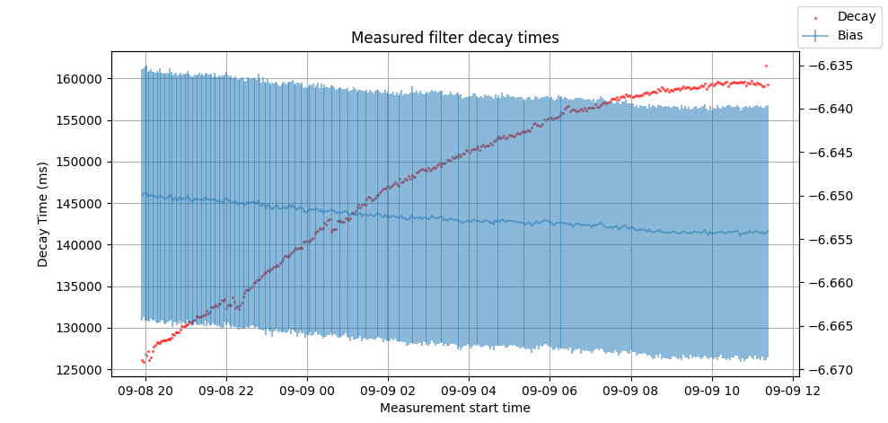
Here are some fun plots featuring a test that was left running overnight near the upper limit of decay time. I also got some data at a few other points this morning, but the longest decay time data is the main feature here.
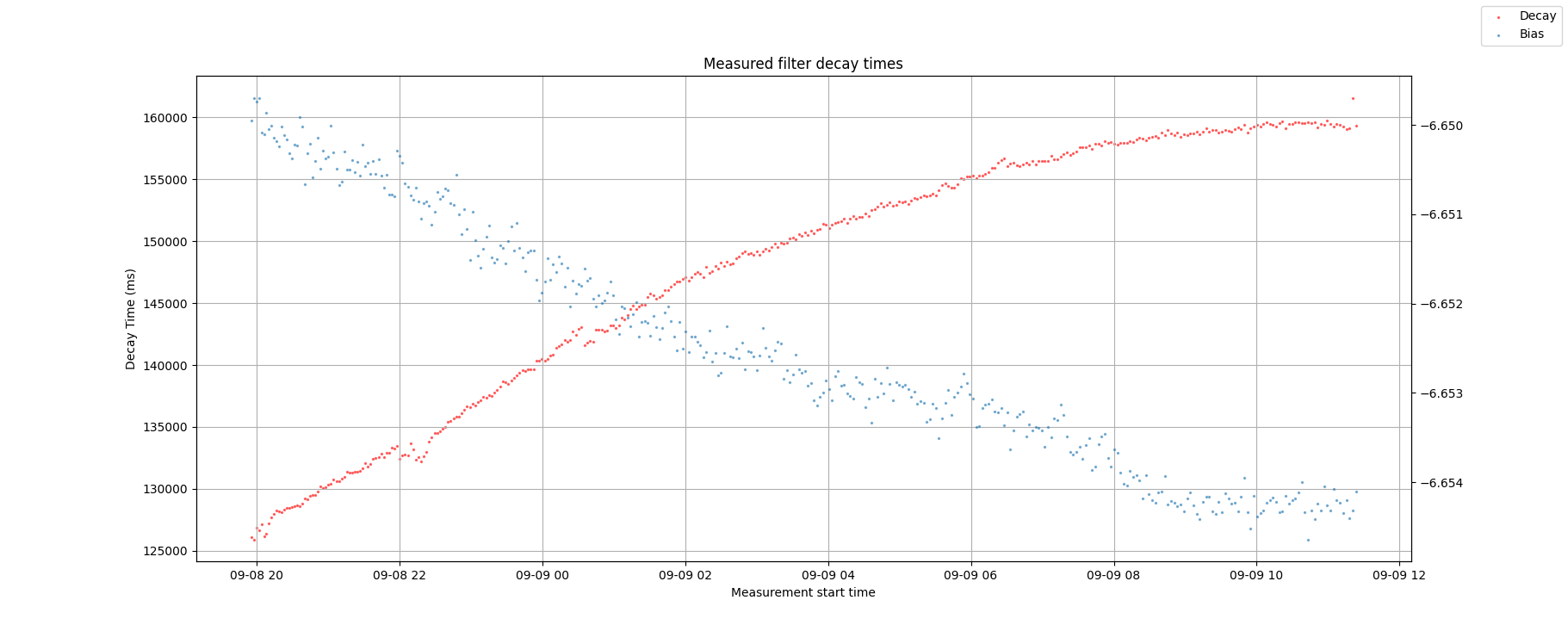
The bias voltage drifted over the course of the night, and seems to have been the primary factor in variation of decay time overnight. There are a few visible step-like changes in decay time that seem like they might be accomanied by steps in the bias voltage, but it's difficult to pick out from the noise. The noise itself seems to have no impact on decay time and is presumably a measurement artifact. Interestingly, the drive in decay time over bias voltage doesn't appear to match the slope of the baseline data taken yesterday.
It is worth noting that the bias voltage plotted here is the average of the maximum and minimum bias voltages measured over the entire duration of the measurement. The errorbars here are huge relative to the range of observed bias voltages:
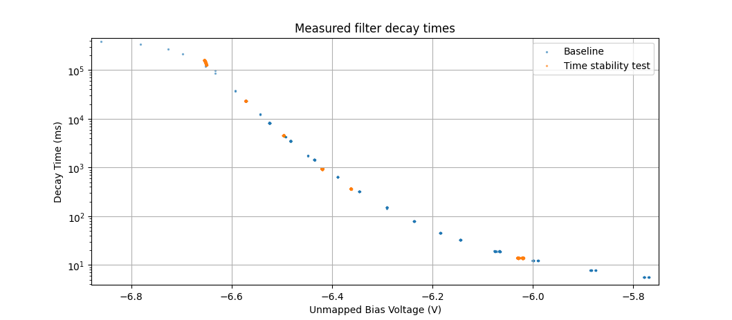
For fun, I put in a 0.47 uF filter capacitor. The one I had in stock was a 1206, and didn't quite fit on the 0805 footprint, so it's soldered to the bypass FET on one edge.
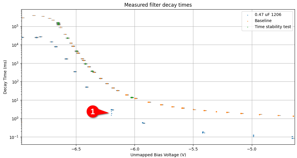 Filter decay times are overall lower, as expected, though it still got up to nearly 30 seconds. The audio interface was less well-behaved during this testing, resulting in a few bad data points (1).
At the lowerst bias voltage, I actually observe the module output drifting below 0 even when the LFSR isn't running. It seems to settle somewhere around -0.32 V as measured by the ES-8. Bringin the bias voltage back up to about -6.86 (ES-8) from the minimum of -6.96(ES-8) causes it to start to recover back to 0 V, and it gets all the way back to 0 somewhere around -6.6 (ES-8). The corresponds to a decay time of around 2 s. It seems like this effect may have introduced some measurement error at higher decay times due to a lower peak voltage decay to a lower minimum voltage. Subsequent measurements seem to reinforce this:
At about 1 s decay time, the slope of the curve on the logarithmic plot looks roughly similar for both 10 uF and 0.47 uF capacitors. Both cases have measurements at about 350 and 1730 ms. The slope is slightly lower for the 10 uF case than the 0.47 uF: -16.3 s/V vs -18.6 s/V. That's closer than I expected, and suggests that barring the strange negative voltage drifting I observed, it's probably feasible to use a smaller value of capacitor and still achieve comparable tuning sensitivity. However, I don't have any 1 uF 0805 capacitors to test with at the moment. I may order some with the udpated JFET part, though.
I also found an issue with the recently-implemented average bias data in the json output - for some reason at higher durations, it was falling outside the min/max range. This makes me wonder if I am somehow mis-counting the number of samles during each measurement. I would expect the error to be more significant at lower decay times than at higher decay times, since a longer measurement would minimize the effect of any fenceposting error. Alternatively, it may be the case that using a single-precision float to accumulated measurements resulted in enough accumulated error to produce bad average values.
Testing by just changing the variable type between float and double seems to confirm this. As a float, it quickly falls out of range of the min and max values. That's doesn't happen when using a double.
That'll have to be it for today. Tomorrow I'll swap in a new 10 uF cap and take more data. Then I'll do the same with a new JFET if I have time.
2021-09-08
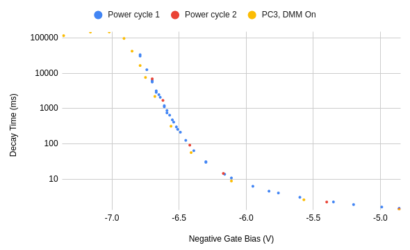
I realized last night that I can measure the gate bais voltage through the ES-8 and cal out its error with the DMM. This way I can have the decay timer automatically include gate voltage without making me manually type it out. Based on a quick measurement at 3 points, the mapping for input 3 on the ES-8 is VDMM = 1.037594*VES8+0.04203, and this appears consistent across power cycles.
Well, the implementation is pretty ugly, but it gets the job done. The decay measurement module now generates json files containing all of its measurements. If the file already exists, then it merges its measurements with the existing measurements, determining whether two measurements are identical by timestamp.
Here's the baseline data taken with the updated measurement module (plotting script and raw json here).
I should probably order the new JFET PN to be sure that behavior is similar. I don't really have much of a digikey order queued up yet, though. For now, at least, I can test with some different capacitors and some of the spare JFETs I have on hand in order to see the impact of part-to-part variation, but I think I definitely need to test with the new part number before locking in a design.
2021-09-07
I can see that the gate bias measured by the DMM and the scope DMM change depending on which are connected and/or powered on. It's not actually too surprising given the ~100k impedances in the biasing network. Normally a change of a few tens of mV wouldn't be a huge issue and could be neglected, but in this case it's significant. To that end, I should probably perform characterization with the DMM powered on since the gate bias is actually changing when I power it off. It may also be prudent to use a stiffer bias network to minimize the impact of stray impedances due to manufacturing variation.
Given the that the DMM powers off after a while, I would like to eliminate its impact on the measurement. I would also like to get my data into python and make the collection a little less tedious. In hardware, I'll need to add a stiffer bias network. In software, I'll modify the decay time to include a field for entering bias voltage and have it store each timestamped measurement in a list that can be written to a json on demand. This will also allow me to observe variation over time for thermal or discontinuity effects as well as exclude junk data caused by audio interface issues. By the way, here's another plot
This one captures the upper limit on decay time.
The updated bias resistors are 7.5k to -12 V and 5.49k to the control voltage based on what I had on hand. This should produce an offset around -5.08 V, although, of course, the -12 V rail isn't a voltage reference. Presumably in the next revision I'll be able to apply the offset as part of the CV scaling circuit to avoid the increased current consumption. I may want to also look into using an onboard reference voltage so that even if I need a calibration trimmer I'll at least not be dependent on the external supply being consistent.
The actual bias range is now -4.91 to -7.42 V. A bias of -6.62 produces about 892 ms decay with the DMM powered, and 930 ms with the DMM not powered. Previously, the decay at -6.62 V was abut 1700 ms, and while I don't have a measurement at that bias with the DMM powered, the new value seems in line with the other measurements. The variation is about 4% between measurement conditions in the new configuration, and should get worse as decay time increases.
At -6.7 V, I see about 3360 ms with the DMM powered and 3515 with the DMM unpowered, for a variation of about 4.5%. I think this is probably adequate for capturing part-to-part variation and characterizing the shape of the bias-to-decay time curve. Next I'll update the timer module to generate json outputs.
Module update taking some time, naturally. json in C++ is hell of tedious.
2021-09-06
Happy Labor Day, comrades. I'll be celebrating by doing some fulfilling and enjoyable labor instead of useful and paying labor.
Today, I'd like to replace the bypass JFET with a BSS138 in order to see how that affects filter performance. I may also look around and see if I can't find a smaller 0805 capacitor to replace the filter capacitor. Smaller capacitor values should behave better over bias and be more reliably in stock.
When replacing the bypass transistor, I'll need to disable the bypass functionality, since the comparator is currently configured to output -12 V for bypass mode, which is the opposite of what I want for a FET. I may want to cut the trace to the gate, since the absolute maximum VGS for the BS138 is +/- 20 V, and with both LFSR's active, the filter input can get up to 9 V, producting peaks of 9 V on the output. With a bias of -10 V on the gate, this gets pretty close to the limit, and these are really just guesses at the TL072's min/max output voltages.
Actually, in the updated design I should probably put the gate after the filter instead of before. With both LFSR's active, the pre-filter buffer will be producing its maximum output voltage, and in bypass mode the comparator will also produce its maximum voltage, so VGS will get all the way down to 0 V. For an NFET to work as a bypass transistor, I need the peak source voltage to be relatively low compared to 9 V.
To that end, I actually want to reduce the pre-filter gain back to 1 so that I can just tie the comparator input to gnd and drive the bypass FET gate at -9 V without worrying about killing it. And also so that I can get relevant characterization data for the next revision.
After those two updates, I'll do a quick test to determine the bounds of the control voltage that produce useful behavior and see about modifying the scaling circuit to give me a little better sensitivity on the knob. Ultimately, I want to allow the control voltage to go all the way to 0 in order to give access to audio-frequency filtering behavior, but for the purposes of characterization, I don't think I need to go that low, so it's worth considering a scaling circuit that gives me cutoff as high as, say, 400 Hz and as decay times as long as, say 5 seconds.
In order to facility re-characterization of the updated filter, I may also want to implement a VCV module that includes a comparator with hysteresis and a gate-length measurement function (the nysthi module measured time between pulses, which is not exactly what I want).
It may also be prudent to try swapping out different JFETs and capacitors in order to characterize variation in the filter across parts. It would be unfortunate to wind up with a control knob that works perfectly for this specific unit and then doesn't work at all on the next one.
After reducing the pre-filter gain to unity and replacing the bypass JFET with an NFET, I find that a gate bias voltage of -6.73 V produces an decay time of about 4.96 s. I see decay corresponding to 420 Hz around -5.6 V. With the current setup it's quite difficult to measure at 0 V, but it looks like around 2.4 kHz.
Leakage through the NFET isn't an issue at all. As for using a smaller capacitor, I'm a little concerned that the JFET will be less well behaved or less tunable at higher rds given the vaguely exponential response to bias, so I now believe that decreasing the filter capacitance would make it harder to tune the filter decay. I'd have to get down to 10 nF to use np0's and get away from the poor tolerance of X7R's.
The 10 uF capacitors I'm using right now have a 16 V rating, which should be plenty against a 3.3 V swing. It might be that a smaller capacitor would provide a more linear ramp due to reduced DC bias variation, but I'm not sure that's an issue. The exponential ramp is fine.
Next I'll go ahead and implement that measurement module so that I can characterize the current configuration. There's no harm in trying out a smaller capacitance later, especially if I go through with trying out different parts to capture part-to-part variation.
I would also like to modify the bias-mapping circuit to yield a range from, say -5 to -7.5 V. That's around 5 times smaller range than the current configuration and still gives some margin around the 5 s to 420 Hz range. I'll probably want to use a passive network to apply a negative offset to the gate. A 137k pulldown to -12 V yields an offset of about -5.06 V, which is close enough. This means the output of the scaling circuit will be scaled down by a factor of 0.58, so I need a range of about 4.3 V out of the scaling circuit, and replacing the 22k input resistor of the scaling circuit with a 75k resistor gets me pretty close. I should have some 75k resistors since this design uses them in the length CV scaling circuit.
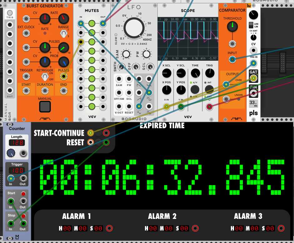
Decay timer is now finished:
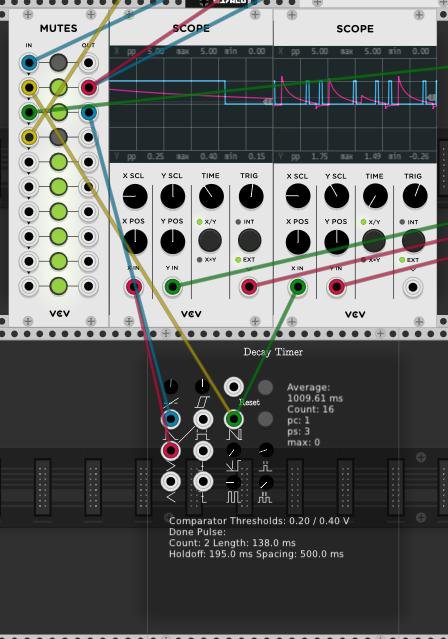
This makes life quite a bit easier. There is a comparator section with configurable hysteresis, over/under gate outputs, and rising/falling edge trigger outputs. The timer section measures the duration of the gates and tracks multiple trials. There is also a configurable pulse output when a measurement finishes in order to retrigger the filter. The last bit is a bit fiddly, especially with delay through the ES-8, but nominally after a measurement finishes it will produce a single pulse to produce a falling edge in the LFSR output, and then another pulse to produce the rising edge that triggers the decay. If it gets out of phase, then the second pulse should be aborted by the start of a new measurement provided that the new measurement starts before the delay between pulses expires (which is where the ES-8 latency can become an issue). I haven't yet tested it with very fast decay rates.
Here's my first sweep using the new measurement module. It works pretty well all the way down to the fasted decay time currently on the knob.
I'm not sure what accounts for the splitting at the upper decay times. I may have power-cycled the rack somewhere in there. It's also possible that I need longer holdoff times when measuring longer decay so that the measurements are more independent. Given the limitations of my DMM resolution, I'd expect some noise at higher decay times, but I would still expect to see monotonic data.
Here are the measurements from both configurations overlaid. Blue is the data taken with the decreased filter gain and NFET bypass installed, and red is the data taken yesterday.
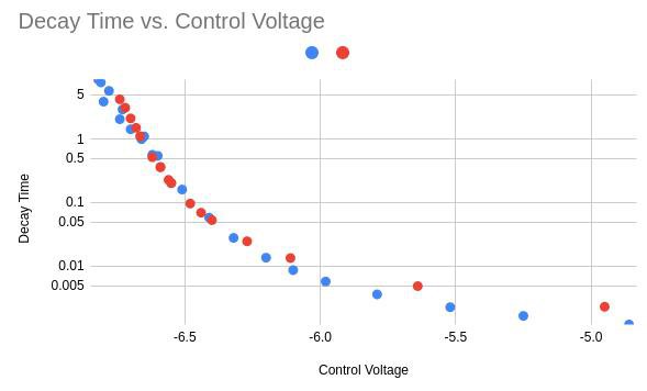
These two line up remarkable less down to 50 ms. It's possible that the difference in measurement techniques accounts for the variation in data, as using an LFO would have prevented the filter from settling before trials.
Interesting note: The decay varies substation depending on whether I have the DMM powered will probing the gate voltage. Disconnecting the unpowered DMM from the ground lead also changes the behavior substantially.
At decay times in excess of 2 s, I'm observing some really dramatic variation. It typically seems consistent over short time spans, but seems to sometimes change quickly to a new duration. I'm not sure if the stepped behavior I'm noticing is real or imagined, though. Right now I'm looking at a test that was sitting around 7-8 s for 10 trials or so, and now seems to be at about 14 s. I don't really have sufficiently granular data collection to say more at this point. I may want to update the measurement module to save individual trials and produce json output on demand.
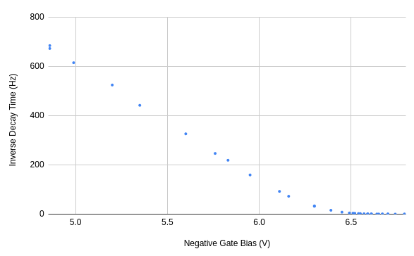
There is a pretty obvious linear relationship between the inverse of the decay time and the gate bias down to 50 Hz or so.
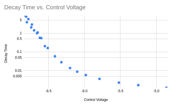
2021-09-05
Starting the day by restoring the pre-filter gain on the rev01 and removing the JFET bias feedback circuit on the rev00. Unfortunately, what I did instead was place a 10k resistor in the rev01's feedback circuit where I had previously removed the 100k resistor. This has resulted in not the desired behavior.
The good news is that the rev00 filter seems pretty well-behaved. Without a working ext-clock, there are limits to how far I can test it, but at the lowest output frequency I could achieve, it seems pretty well-behaved, indicating that the guard ring isn't really necessary as there are no board-associated leakages significant enough to cause problems.
Given that it's not too hard to get a square wave with a negative lower voltage by just adjusting the filter quickly, I think that the bypass option remains necessary. I'll need to test performance with a BSS138 in place of the JFET to ensure that the increased drain-source leakage in the off state isn't an issue.
After fixing the error on the rev01, things seem to be mostly working. Things are even relatively well-behaved with both LFSR's engaged for a pre-filter waveform voltage of 0 - 9 V. The next thing I'd like to do is characterize the filter decay time as a function of control voltage to get some sense for what kind of correction curve I need to use to get better control over the longer decay times.
In order to do so, I need a means of measuring the output pulse duration. My old analog scope isn't really suitable for measuring long pulses, which is the data I'm really interested in. That said, I can make the nysthi expired time module in VCV work along with a comparator and a couple edge detectors. Since I'm concerned with long pulse widths, this should be fine.
Decay time was measured using VCV Rack and defined as the time between the filter output going high and dropping below 0.2 V as measured with the software. A comparator (without hysteresis) was used to generate a gate signal corresponding to the decay time. The gate signal was passed to an pulse generator, which in turn triggered a timer module. The pulse generator served to prevent false pulses due to the lack of hysteresis, but prevented measuring shorter decay times.
Short decay times were instead measured by driving the module with an LFO and visually aligning the compator gate output with the negative edge of the filtered signal. When the two were aligned, a single period of the LFO corresponded to the duration of the comparator output, and could be used to compute the decay time.
The JFET gate control voltage was measured by uncalibrated DMM at the cutoff control test point (the output of the cutoff gain control op-amp). This should be suitable to at least determine the shape of the curve relating decay time to control voltage. The DMM has 10 mV precision on its display, and at long decay times, substantial variation is observed over changes of 20 mV, so the measurement quality is expected to be relatively poor.
Initial results look relatively promising, though:
The curve clearly isn't quite exponential, though at high decay times it might be a good approximation.
2021-09-04
At this point, it would be helpful to have the external clock functionality working so that I can get a better look at step response. I also intend to look into options for extending the lower frequency range in software, but I don't really want to deal with that right this second, and I think it's al ess essential feature - rhythmic behavior, I think, is more likely to be accessed using an external clock to permit synchronization.
I have no idea what I thought I was doing with the rev01 jack detect circuit. I am honestly clueless. As it stands, this implementation isn't even close to being remotely functional.
![]()
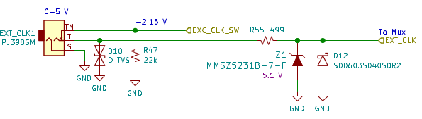
In the rev 00 design, the switch pin was biased at -2.16 V, and so could briefly place that voltage on any connection before breaking the switch. The high bias resistances made that unlikely to be a significant issue, but I'm aware that other designs have had issues with this approach in the past (albeit without the high impedance between the bias and the switch pin). In the original implementation, it was intended that a PFET would be switch on when the switch pin and signal pin were connected due to the negative bias voltage. When the two were disonnected and a clock signal driven on the clock pin, it was expected to put >= 0 VGS on the PFET, causing it to switch off and toggle a clock select select multiplexer. In practice, I saw the external clock duplicated on the clock select signal.
In the rev01 I intended to use a simpler design with the clock switch pin normally biased at 0 V. The idea was that the switch signal pin would be pulled to 3.3 V, and the switch pin pulled to -12 V with resistors selected to provide a 0 V bias point. When the two were disconnected, the switch pin would be pulled to -12 V, switching a PFET on later down the line. Meanwhile, the clock pin would be pulled to 3.3 V, allowing operating with an open-drain clock as well as a push-pull clock. Here's what I actually did
The jack switch is pulled down. That is all. I think at some point I realized I could make with work with an NFET by biasing the pin above 0 V to switch the FET on, and having it pulled down when disonnected to switch the FET off. This is marginally less elegant than biasing at 0 V, but reduces BOM complexity by eliminating PFETs from the design, and should be generally safe since 1.5 V through high impedance shouldn't hurt anything that would find use in eurorack.
Regardless, that is not what I did. At all. Also I would like to call attention to the current over-voltage protection scheme, which uses a zener diode to clamp the clock input to 5.1 V. The rev00 design used a 5V-tolerance multiplexer, and the rev01 design uses a 5V-tolerant CPLD, so this is technically legal. I'm pretty sure I could just drop down another NFET and get rid of the two protection diodes, though, reducing BOM complexity, simplifying the CIB, and providing more elegant protection. The main drawback is that an open-drain clock is limited by the trade off between current consumption and switching speed. For audio frequencies, this is no problem at all. It might start to become more of an issue in the 10's of MHz, though, which could limit, for example, video synthesis applications. That's not really a requirement of the design, though. I think the issue could be resolved by BOM replacements (smaller pullup resistor and maybe a different NFET with a lower threshold voltage), which could be necessary anyway to increase filter cutoff frequencies and use faster op-amps on the output (assuming a pin-compatible solution exists. As I said, video compatibility is not a Requirement).
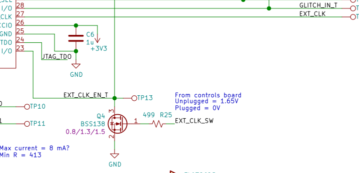
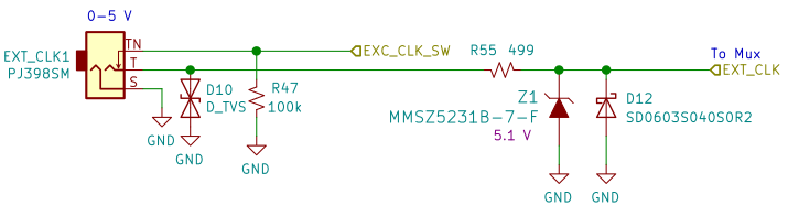
The first step, now, is to just add a 100k pullup to the ext clock pin, which shouyld make the clock select work. 1.65 V is pretty close the max value of 1.5 V for the FET threshold, but it's still above, so it should be fine, especially since it won't take a lot of current to pull to 0 V through the 100k pullup on the clock select.
Okay, hold up. 1 second.
I just checked to make sure that it's currently behaving as I described, and I find that the clock switch is at 2 V with nothing in the jack, and 0 V with a cable in the jack. Is it possible that I enabled a pullup in the CPLD? I don't see a bodge on the module currently.
After removing the cable, the switch voltage remains at 0 V. This is really strange. With 100k pulling the switch pin down, it shouldn't be able to float anywhere.
After power-cycling the module, the switch pin returns to 2 V (really, 2.25 V). This corresponds to the behavior I would expect from a 46k pullup, which seems reasonable for he CPLD. From what I can tell, though, I don't have pullups enabled. DC resistance to ground it 100k, so it can't be some sort of connection issue. DC resistance to 3.3V is also 100k. With the jack connected, I still see 106k to 3.3 V and ground, which is surprising. The clock pin itself also seeings 100k to 3.3 V and ground, and see about 200k to the switch with the jack connected. With the jack disconnected, I see the expect 500 ohm (measuring on the main board).
Unless the FET is somehow damaged, I don't see any way for this to be the case. The switch pin, with the jack connected, has a 100k pulldown to ground and it otherwise connected only to the FET gate. I suppose it could be measuring resistance to 3.3 V via ground, though. DC resistance from 3.3 V to ground is on the order of 6k. I think that's the most likely scenario here, so this doesn't tell me anything about the appears of 2 V on the switch and clock pins.
Strangely, I am now seeing the 2 V persist through jack cycles. When I connect to 0 V via an ES-8 output, it returns to ground and stays there. I also see 2 V present on the clock pin when powering the unit with the jack connected. In that case, the pin would be floating, and so a pullup opposing a pull down doesn't explain the result.
This is quite strange, but I'm going to go ahead and proceed with adding the 100k pullup and see what happens.
After adding the missing pullup, the external clock functionality seems to work except that there's some kind of noise or intermittent behavior going on. It seems to get worse as I decrease the clock amplitude until I drop below the CPLD's threshold. There is a hell of a lot of ringing on the clock, but filtering it before bring it out of the ES-8 doesn't seem to help at all. If anything, it seems to get worse without the ringing (and with lower slew rate). I can shift the clock's lower voltage below 0 so that it gets clipped by the protection diode, and the issue improves a little bit as the lower-end ringing decreases.
There may be a lack of hysteresis on the CPLD inputs causing it to be very sensitive to noise. I can send a pretty clean triangle wave in and get very bad noise performance. A FET buffer could provide protection against out of range voltage and help clean up the signal edges some. A schmitt trigger would provide hysteresis, but would not provide voltage protection and would also increase the BOM complexity, a situation I would kind of like to avoid. I should try adding a FET buffer first to see if that helps at all.
The buffer certainly helps. I used a 10k pullup rather than 100k, and with a square wave I get a pretty clean outputup to around 12 kHz, at which point the signal gets LPF'd enough to stop exceeding the gate threshold. This appears to be a limitation of the ES-8, as I see the same just looking at the output directly.
If I probe the post-buffer signal, I get some crackling, and if I use as triangle wave I also get some pops, though it's not as bad. I think it would be nice to be able to drive this with signals other than square waves, though, so I think some hysteresis is warranted. At the same time, I'm not sure if it's reasonable to put the hysteresis after the buffer. The buffer output is essentially digital, so any popping due to lack of hysteresis should already be present at that point. It seems that the capacitve loading of the probe is affecting the noise, as it changes character when I switch the probe gain.
It might be best to put this off until the next revision, and design rev02 to include the option for playing with hysteresis and filtering more easily. This bodge is already a little fragile. For now, I think this solution is adequate.
Now I have what I need to return to the coupling filter. I've turned the cutoff way down without going into bypass mode, and I'm feeding a DC into the external clock so that the LFSR isn't switching. I can see the output dropping very gradually. Though I haven't time it yet, the ES-8 reading has dropped about 0.04 V in the past several seconds, which seems like a good sign.
With 0 V out of the LFSR, I can see the output very gradually dropping below 0 - by about 10 mV in 39 seconds with the cutoff turned as low as it will go without enabling bypass. Of course, I can turn the cutoff back up to quicly drop the output back to 0 (or -037 mV as the ES-8 reports).
Bringing the output high again, the initial output voltage is 1.532 V as reported by ES-8. After 4 minutes, that has dropped to 1.476. It's safe to say I can get the cutoff arbitrarily low. It might be expected that at low duty cycle this would drift over time, though very gradually. It might still be worth keeping a bypass circuit to ensure perfect logic operating without having to worry about periodically clearing the offset. Since the offset only falls when the LFSR output is high, a low duty cycle should drift more slowly than a constant. A high duty cycle should drift more quickly.
I left it running at low duty cycle for 7 or 8 minutes, and when I cam back the sequence had changed. It didn't seem to have drifted much.
I would like to modify the rev00 filter and compare performance to see what impact the guard ring might have. I also need to modify the rev01 filter to put back the pre-filter gain and see how that performs. I'm curious to see how the filter performs with a smaller capacitor, and might look into trying one if I have one in a suitable package.
With a slow clock rate (0.5 Hz), it is not too hard to wind up with an offset binary waveform in the process of trying to dial in a slow ramp. I guess I had overshot the mark quite a bit. It's possible to do as is, but a bit fiddly. I tried just touching the knob and not quite turning it down, and the decay dropped from about 1 second to more like 250 ms. It might be worth investigating the possibility of adding a logarithmic converter order something to get better resolution in that range. Alternatively, maybe I could just get a knob with a different taper. This will require sitting down to think about what exactly I need to do in terms of mapping the knob output. For now, the headache insists I'm done for the day.
2021-09-03
Just a quick note: JFET gates are PN junctions. When I put 12 V on the bypass JFET, I was forward-biasing the shit out of it.
Simulation seems to show that a random NFET will work fine for a bypass transistor. I'm not sure if drain-source leakage is captured in the simulation, though. Of note: the mmbf4391 in the design is obsolete. The replacement mmbf4391lt1 seems to have a worse leakage spec of 1 nA at 15 V and 1 uA at 100 C. The bss138 NFET I've been using in this design is 100 nA at 30 V, 500 nA at 50 V, rising to 5 uA at 125 C. The performance over temperature is a bit better, sure, but at ambient it's substantially worse than the JFET. Still, with the gate at -10 V rather than 0 V, and with a much lower VDS, performance might be fine in this application. The spec'd leakage at 30 V corresponds to 300 Mohm. My tea is done steeping, and I need to go do some actual paying work.
The PN4391 model I was using may not have been a good fit for the MMBF4391. I downloaded some newer models at https://www.interfet.com/jfet-datasheets/standard.jft.
I've modified the simulation to just look at the relationship between control voltage, VDS, and the JFET resistance. I see a pretty significant dependence of the resistance curve on VDS for larger values (1, 2, 3 V), but it looks a bit more consistent in the range of 0.1 to 0.5 V. This makes some sense - the linearizing feedback is based on the small-signal model for rds .
Even in the range of 0.1 to 0.5 V, there is a substantial variation in the control voltage where rds exceed 100 k - about 0.1 V between each. This is pretty significant when the control voltage difference between 1k and 100k is also 0.1 V. Overall, I observe the rds at a given control voltage decreasing with increasing VDS. at 0.1 V, the control voltage range for 1k to 10 M is -9.236 to -9.3 V, a difference of 64 mV.
Since resistance increases substantially as VDS drops, the filtered waveform has a hard time actually getting down to 0 V. This makes envelope functionality fucking blow, basically. The envelope drops rapidly and then levels off somewhere above 0 V, so it spends most of its time at a constant voltage below the peak. It's like an ADS without the R. It just sustains forever.
If I abandon the linearizing feedback path something interesting happens, though. Over a control range of -4.4 to -4.6 V, I see the following:
This seems extremely well-behaved. I'm not sure this would hold up in the real world - for one the last case where there appears to be no cutoff is just the capacitor swinging back and forth be 0.1 V with no integrated error of any sort, and no leakage of any sort. That is certainly not realistic.
The rds of the JFET should depend on its threshold voltage, and I don't expect that value to be consistent from part to part. Combined with the extremely small tuning voltage range of 0.2 V, this circuit would almost certainly require some calibration. Does the JFET threshold voltage vary with temperature? It seems pretty likely.
It's probably worth experimenting, though. If behavior is consistent enough, then it should be possible to put down a little pot for calibration and get some decent envelope behavior.
Finally, at larger voltages the waveform becomes very asymmetric. This seems reasonably desirable for envelope behavior, but I'm not sure what it would sound like at audio frequencies. The control looks more linear here, though.
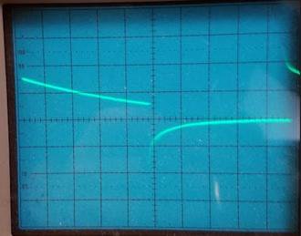
Initial tests after simply removing R33 look extremely promising. The full control voltage range is presently -10 to 0 V, which the op-amp cutting off the bottom of the knob's range. The knobs was adjusted by awkwardly reaching around the back of the rails with one hand with probing the output pin on the module with the other hand, so I didn't have a lot of dexterity to spare. Even so, I was able to dial in decent performance relatively easily. I was surprised to see a decent square wave coming out without engaging the bypass circuit, which is also quite interesting. The final picture was taken at about 50 ms per div, with the lowest frequency I was able to get out of the module. It looks like the decay would have been about 200 ms. At that scale, the knob did get a bit fiddly. I expect that with a better angle and a more constrained control voltage range it would be completely managable.
2021-09-02
Starting work on debugging the output coupling filter issues. Although the buffer topology has changed, this shouldn't substantially impact filter behavior, and the simulation confirms this. Probing the output of the first buffer directly (at the coupling capacitor), I see an unusual slope in edges of the output waveform:
[I didn't take a picture]
This slope vanished when I remove the coupling capacitor, suggesting that the op-amp isn't at fault. I've been able to heard the output waveform from the capacitor since building this unit, which wasn't the case with rev00. This makes me suspect the capacitor itself may be an issue. My DMM's fuse is blown, so I can't do any capacitance measurements at the moment, but I don't see any DC resistance through the part.
I don't believe the behavior I was seeing could be caused by instability of the op-amp. I would expect the capacitor to provide decent isolation between the op-amp and the rest of the circuit, so it's not immediately clear to me what could be causing this issue. The bypass JEFT is still present. Could the transient current through the capacitor be too much for the op-amp somehow?
The simulation is using an OP27 since I was having issues with the TL072 model. I'm seeing peak currents around 35 mA at the highest cutoff frequency. Things look pretty reasonable at the intermediate cutoffs I'm examining though. Interestingly, in bypass mode I'm seeing between 17 and 35 mA out of the op-amp, which is surprising. It seems like 15 of that is going through the gate of the bypass JEFT Q1, and the other 0-15 is going through the drain JFET Q2. Bypass mode is supposed to align with the lowest cutoff frequency, which should also be the highest resistance of Q2, so I don't expect to see any substantial current through it in that state. Instead it has a resistance around 300 ohms when the output waveform is high.
This seems related to the linearizing feedback path (R33, R34). I'll need to review this application some, I think. I'm seeing quite a lot of variation in the effective resistance of the JFET with variation in the waveform voltage.
I still don't have any idea why this is behaving substantially different than the rev00 prototype, though, as the circuit is essentially unchanged. The waveform levels are higher than the original, so maybe that's causing increased current draw during transients and overloading the op-amp. That shouldn't be an issue at intermediate cutoff values where the current shouldn't be getting above 10 mA or so, though.
Replacing the capacitor with a new one didn't resolve the issue, but it did change the behavior of the circuit substantially. The slopes in the op-amp output are now much more dramatic, and the filter output decays more slowly.
I suppose the next thing I might try is removing R16 to make the op-amp act as a buffer, lowering the peak output voltage to 1.65 V. When I look at the filter output, I need a knee somewhere around 2 V (though this varies with cutoff configuration). The rev00 seems to have a similar knee, though it's near the peak of the waveform and less pronounced.
With the reduced gain, everything behaves quite nicely. The MMBT4391 has a cutoff voltage between -4 and 10 V. In the simulation, I see the gate voltage ranging from -7.5 to -2.3 V depending on the cutoff selection, so I suspect that the increased waveform voltage is pulling the JFET gate voltage high enough to cross that threshold. I still need to review the application of JFETs as variable resistors with this in mind, but I suspect that this is my issue. I may then want to actually attenuate the waveform before filtering in order to imrpove linearity and gain access to higher JEFT impedances for lower cutoff frequencies.
I originally moved the buffer to the end of the signal chain so that I could create a guard thing around the output side of the filter capacitor and eliminate leakage through the PCB or uncleaned flux. I suspect that in the current implementation, the JFET impedance is always going to be much smaller than any such leakage current.
In simulation, I'm seeing the JEFT gate voltage increase substantially when the filter is bypassed. At the same time, I see the minimum op-amp output voltage jump well above 0 V - about 0.75 V. The output at the op-amp is 0 V, so this is a 0.75 V drop across the 25-ohm output resistor, for about 30 mA. I'm seeing the bypassed waveform on the gate of the bypass JFET, which is strange. The bypass JFET is quite warm to the touch - enough to be painful after a couple of seconds.
This does not appear to be the case on the rev00, though the pre-filter waveform never drops all the way to 0 V due to the lack of output enables on the LFSRs. More JFET issues to study.
I'm going to need to add a gain stage after the filter regardless of whether I attenuate the waveform prior to the filter. It may still be possible to create a guard ring from a non-inverting amplifier configuration since the inverting input will still be at the same voltage as the non-inverting input.
Unfortunately, I didn't leave myself any pads to add gain after the filter in this revision. Also wait what? In this revision, the JFET feedback is taken off the buffer output. Is that legal? In simulation, it seems like this has the desired effect of reducing the minimum attainable cutoff frequency. I guess that makes sense. That was always about controlling the gate bias.
In the perfect world of the simulation, using the buffer to provide the bias feedback drops the 3 dB cuttoff with knob at 28% from about 6.5 Hz to about 4.5 mHz, and at this point I have to assume there are leakages not being simulated. It almost seems like it's not decaying to 0, though, which would be a concern for trying to use it as an envelope. The main part of the transient is still pretty short, dropping from 1.65 to 0.6 V in 0.1 s, but then over the next 0.9 s it only drops another 0.1 V.
In fact, if I drop the input pulse to 0.5 V, then at lower enough cutoff it just sits at about 350 mV.
It's probably worth considering the possibility that this approach to filtering isn't worth pursuing. The variable cutoff doesn't really produce an audible difference. With a lot of reverb it can become audible as basically a change in volume, but I don't think that's an important effect. The main goal of providing a variable cutoff was to allow the output to be used as sort of an envelope when the module is operated at low frequencies or with an external clock. If the filter can't be used to produce a decent envelope signal, then it's a lot of complexity that doesn't really add anything to the module. A switch and be used to select between AC and DC coupling.
The reason for using voltage control was to avoid routing the audio signal all the way up to the top of the module through a potentiometer and then back down to the bottom of the module. Given that the signal is LPF's to remove above-audio frequencies prior to the AC coupling filter, it might be accepable to route back and forth across the module. The main concern, I think, would be coupling the LFSR clocks. It should be possible to just route it on the other side of the board and/or away from the LFSR clocks, though. Coupling into other controls might be a concern, as it would have to go through the whole CIB and back to get to the knob.
Rev 00
2019-12 through 2020-07
TODO: Summarize rev 00 development